Nand Gate In Cadence
Layout nand virtuoso gate cadence Nand gate cadence Nand cadence virtuoso gate lvs layout stack problems vlsi schematic integrated circuit
NAND-gate| Digital Logic Gates || Electronics Tutorial
Nand cadence virtuoso fig48 Nand cadence virtuoso buffer vlsi simulation inverters tb Lab 03 cmos inverter and nand gates with cadence schematic composer
Ee4321-vlsi circuits : cadence' virtuoso ultrasim vector file simulation
Hierarchical virtuoso lab5Layout nand gate cmos cadence lab simulation xor 421l ee tutorial through adder generated schematic going while below were Nand-gate| digital logic gates || electronics tutorialCadence schematic gate layout nand cmos assura verification.
Cadence nand gate virtuoso using simulationGate nand input three electronics gates logic digital tutorial figure above shows Cadence virtuoso:: layout of nand gate || part-2.Ece429 lab5.

Gate designs: design nand gate using cmos
Inverter nand cadence nmos pmos cmos multiplierLab 6 ee 421l spring 2015 Simulation of basic nand gate using cadence virtuoso toolLayout input nand.
Nand finfet 7nm geometries 9nm respectively4-input nand Cmos 2 input nand gateLayout geometries of 7nm finfet nand gates with l g =7nm and 9nm.

Cmos nand layout cadence
2: complementary cmos three-input nand gate.Nand layout cadence virtuoso gate tool using 1: a 2-input nand gate layout designed in cadence virtuoso.Integrated circuit.
Layout of nand gate using cadence virtuoso toolCadence tutorial -cmos nand gate schematic, layout design and physical Nand gate circuit and simulation in cadenceCmos nand complementary.

Nand cmos gate input layout microwind pspice
.
.


2: Complementary CMOS three-input NAND gate. | Download Scientific Diagram

CMOS 2 input NAND gate | All For Students

Layout geometries of 7nm FinFET NAND gates with L G =7nm and 9nm

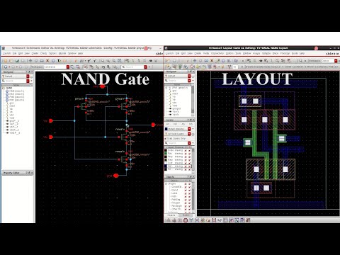
Layout of NAND Gate using Cadence Virtuoso Tool - YouTube

NAND Gate circuit and Simulation in Cadence - YouTube

4-input Nand

1: A 2-input NAND gate layout designed in Cadence Virtuoso. | Download
Cadence Virtuoso:: Layout of NAND Gate || Part-2. - YouTube
